July 8, 2017
I previously wrote shortly about atomic force microscopy (AFM). With this amazing tool, surfaces can be mapped with a resolution of several nanometers, that is several tens of atoms. Imaging the surface topography is maybe the most common use of an AFM but the technique offers many other possibilities ranging from nanomechanical measurements to nanoprinting. I have been in contact with AFM since 2008 and many manufacturers have introduced stunning new applications since then. What I want to write about today is 3 very recent advances in the AFM technology that are already commercially available or will be soon. Please note, the list is far from being a result of a complete review.
1- Video-Rate AFM
The first AFM breakthrough I would like to discuss is the Video-Rate AFM, presented by Asylum Research (Oxford Instruments). The technology is only possible in their premium product Cypher VRS™ for now. Regarding the video-rate principle: an AFM tip scans a surface line-by-line or pixel-by-pixel and the resulting image is traditionally static. It is just one image, collected usually in several minutes. The image can show a surface of let’s say 50 nm x 50 nm in size but also of 50 micron x 50 micron (a million times larger), depending on your needs. In accord with its name, Video-Rate AFM can generate these static images so fast that they form a real-time video. As an AFM insider, I cannot express how amazing and useful this can be: you can monitor how crystals are formed, how a DNA helix opens up, how a protein or a cell moves and many more phenomena both live and nearly at the molecular level. It is a significant step on the way to monitor individual molecules or atoms, for example during a reaction. You can see some inspiring videos under this link. This video for one shows how collagen fibers are assembled on a mico surface in real time:
Detailed info: What makes this technology possible is (1) Much smaller cantilevers that can vibrate much faster than the usual ones and (2) The company’s blueDrive™ photothermal cantilever excitation method, that makes these fast vibrations possible.
2- OT-AFM
The second exciting technology named OT-AFM comes from JPK, who is based in Berlin (They are actually my neighbors, ~500m from where I live). The researchers and engineers there combined an AFM with “optical tweezers“, which differ from normal hair-removal tweezers in terms of (1) optical tweezers can hold and move very, very small particles – 50nm to 10 microns according to JPK. (2) The particles are trapped not between two physical walls but in a light field. Have a look at the image below (taken from jpk.com):
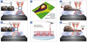
What makes JPK’s product exciting is its ability to move small objects with a nanometer precision while being able to run standard AFM measurements simultaneously. A good example I have seen in their webinar is measurement of the interactions between two cells in the absence and existence of a third cell, which is moved by, yes, optical tweezers! If you are interested, here is the related webinar.
3- AFSEM™ (AFM + SEM)
The third exciting product I came across is a result of the collaboration between GETec and Nanosurf. This product named AFSEM combines an atomic force microscope and a scanning electron microscope, SEM (Click for a very good video explaining this method). SEM gives real time images of surfaces with resolutions usually lower than an AFM can. However, the strength of the SEM is that the generated images are live and the area that can be observed is much larger compared to AFM. Another great advantage of SEM is that once it is coupled with an EDX, elemental analysis of the surface is possible. It means that you can “see” where and on what kind of elements your AFM cantilever and tip are. Subsequently, the images generated by AFM and SEM can be combined to give a much deeper insight into the material and surface under investigation. By the way, in a standard AFM, you can see the cantilever as well with a light microscope but the resolution is no match to an SEM. You can watch GETec and Nanosurf’s webinar here. The introduction video is pretty cool as well:
Although placing an AFM in an SEM is not really a new idea and there are other manufacturers doing this, AFSEM seems to be one a good and well-established AFM-SEM combination. Technically, placing an AFM in an SEM is not trivial because SEM requires high-vacuum and many traditional AFM instruments probably would not work at vacuum as some parts in the AFM device would be over-heated in the absence of air. A more principle problem is the detection of the cantilever bending: usually a laser beam is used to detect how much a cantilever is bent but the AFM unit in AFSEM is laser-free, which I think is brilliant. Side-note: SEM is also not a “traditional” microscope because it uses “electrons” instead of light to “observe” a surface.
The advances in nanotools above are no exception: nanotechnology is advancing way faster than ever! I think nothing physical is impossible as long as we put effort to control phenomena in atomic scale (of course only for now. Although hard to imagine now, mankind will one day control even subatomic particles, gravity waves and things that we are not even aware of now. This is the topic of another post, though). For now, what machines can do is quasi-nano and micro 3D printing, which will most likely lead to another revolution in manufacturing of hi-tech goods. I will write about these technologies and their possible perks soon.
Dr. Çağrı Üzüm
Disclaimer: This is a personal blog. I write about things that I find exciting and think are worth sharing. The content was not influenced by advertising or sponsorship. There may be other great products from other companies that I am not aware of (actually I would appreciate if you could write to me if you know any).

This work is licensed under a Creative Commons Attribution-NonCommercial 4.0 International License.